Journals > > Topics > Special Issue for Light Field Manipulation and Applications
Special Issue for Light Field Manipulation and Applications|26 Article(s)
Fast Computational Algorithm for Large Size Computer Generated Fresnel Hologram by Periodically Extending Integral Term
Jianyun YAO, Xiaolin YING, Fuyang XU, Qiong WU, Haihua ZHANG, and Yong LI
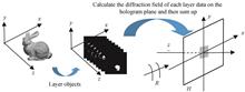
The phase and amplitude of object light field can be simultaneously recorded by hologram, and all the depth cues required by human eyes can be provided by its reconstructed image. Therefore, holography is considered as an ideal true three-dimensional (3D) display technology. With the development of computer technology and electronic technology, computer-generated holography appears. The real and virtual scene can be recorded and reconstructed by Computer-Generated Hologram (CGH). It is more suitable for 3D display. However, the huge amount of computation is one of the bottlenecks to realize high-quality CGH based 3D display. Improving the computing speed is an important direction in the application research of CGH based 3D display. Layer-based algorithm is a critical approach to generate CGH. The three-dimensional object is divided into several parallel planes. Then, the complex amplitude diffracted by each layer of object onto the hologram plane is solved by Fast Fourier Transform (FFT). The complex amplitudes are superposed to form the complex amplitude of object light field on hologram plane. Finally, the hologram is obtained by interfering it with the reference light. The calculation speed is effectively improved, because FFT is used. However, the sample frequency of object plane and hologram plane is constrained by sampling theorem. The interpolation operation of data is adopted to archive this constraint. It reduces the calculation speed, especially when the aspect ratio of object plane or hologram plane is large. The mathematical model of Fresnel diffraction consists of integral term and coefficient term. The integral term of discrete object light field is a discrete-time Fourier transform, which is a periodic function. According to the theorem of digital signal processing, spatial interpolation leads to spatial frequency domain expansion and the spectrum is the periodic expansion of original one. Generally, a low-pass filter is used to filter the unexpected components. Fortunately, the human eye acts as a low-pass filter in 3D display. We can sample the object plane with human eye resolution and calculate one period of integral term. Then, obtain the integral term of hologram plane by periodic expansion. The computation amount of integral term is reduced. Moreover, the coefficient term can be decomposed into two independent parts: row coefficient and column coefficient. We can calculate one row and one column coefficients separately and then combine them into complete ones. The amount of calculation is further reduced. A novel fast algorithm is proposed to improve the computing speed of large size CGH, according to the characteristics of layer-based computer generated Fresnel hologram model. First, complete the following calculation for each layer. 1) Calculate the coefficients of row and column respectively. 2) Calculate a period of the integral term by using the FFT. 3) The calculated integral term is periodic expanded on the hologram plane, and the distribution of the diffraction field on the hologram plane is obtained by multiplying the integral term of each sample point and the coefficient which formed by the combination of the row and column coefficients of the sample. Then the diffraction fields of all layers are summed up and interfered with the reference beam to obtain the hologram. Experiments were carried out to verify the algorithm. Firstly, two holograms were generated by traditional algorithm and proposed one separately. The reconstructed images were compared. No difference was found. Secondly, the reconstructed images under three different viewing angles were taken by the camera. The occlusion relationship between the object and the background is correct. Continuous parallax changes can be seen when human eyes move. Thirdly, the reconstructed images at different distances were inspected. The depth information was reconstructed correctly. Fourthly, the relationship between reconstructed image quality and layer interval was inspected. When the layer interval meets the human eye resolution, the observed reconstructed image is continuous in each viewing angle. When the human eye resolution is not met, the layered reconstructed image is likely to appear in large angle tilt observation. Finally, the computing speed of different size of hologram was inspected. The experimental results show that the larger the hologram size is, the faster the proposed algorithm is. The number of layers has no effect on the speed improvement multiple of the proposed algorithm. When the sample point of volume is 1 174×1 174×41 points, and the hologram resolution is 11 700×11 700 pixels, the calculation speed of proposed algorithm is 13 times higher than that of traditional algorithm. In summary, the proposed algorithm not only ensures good reconstruction effect, but also significantly improves the computing speed of computer-generated Fresnel hologram. It has a good performance in the calculation of large-scale holograms. Further, after calculating one period of the integral term, the subsequent calculations are independent of each other. This makes it possible to further improve the computing speed of hologram by using parallel computing. The phase and amplitude of object light field can be simultaneously recorded by hologram, and all the depth cues required by human eyes can be provided by its reconstructed image. Therefore, holography is considered as an ideal true three-dimensional (3D) display technology. With the development of computer technology and electronic technology, computer-generated holography appears. The real and virtual scene can be recorded and reconstructed by Computer-Generated Hologram (CGH). It is more suitable for 3D display. However, the huge amount of computation is one of the bottlenecks to realize high-quality CGH based 3D display. Improving the computing speed is an important direction in the application research of CGH based 3D display. Layer-based algorithm is a critical approach to generate CGH. The three-dimensional object is divided into several parallel planes. Then, the complex amplitude diffracted by each layer of object onto the hologram plane is solved by Fast Fourier Transform (FFT). The complex amplitudes are superposed to form the complex amplitude of object light field on hologram plane. Finally, the hologram is obtained by interfering it with the reference light. The calculation speed is effectively improved, because FFT is used. However, the sample frequency of object plane and hologram plane is constrained by sampling theorem. The interpolation operation of data is adopted to archive this constraint. It reduces the calculation speed, especially when the aspect ratio of object plane or hologram plane is large. The mathematical model of Fresnel diffraction consists of integral term and coefficient term. The integral term of discrete object light field is a discrete-time Fourier transform, which is a periodic function. According to the theorem of digital signal processing, spatial interpolation leads to spatial frequency domain expansion and the spectrum is the periodic expansion of original one. Generally, a low-pass filter is used to filter the unexpected components. Fortunately, the human eye acts as a low-pass filter in 3D display. We can sample the object plane with human eye resolution and calculate one period of integral term. Then, obtain the integral term of hologram plane by periodic expansion. The computation amount of integral term is reduced. Moreover, the coefficient term can be decomposed into two independent parts: row coefficient and column coefficient. We can calculate one row and one column coefficients separately and then combine them into complete ones. The amount of calculation is further reduced. A novel fast algorithm is proposed to improve the computing speed of large size CGH, according to the characteristics of layer-based computer generated Fresnel hologram model. First, complete the following calculation for each layer. 1) Calculate the coefficients of row and column respectively. 2) Calculate a period of the integral term by using the FFT. 3) The calculated integral term is periodic expanded on the hologram plane, and the distribution of the diffraction field on the hologram plane is obtained by multiplying the integral term of each sample point and the coefficient which formed by the combination of the row and column coefficients of the sample. Then the diffraction fields of all layers are summed up and interfered with the reference beam to obtain the hologram. Experiments were carried out to verify the algorithm. Firstly, two holograms were generated by traditional algorithm and proposed one separately. The reconstructed images were compared. No difference was found. Secondly, the reconstructed images under three different viewing angles were taken by the camera. The occlusion relationship between the object and the background is correct. Continuous parallax changes can be seen when human eyes move. Thirdly, the reconstructed images at different distances were inspected. The depth information was reconstructed correctly. Fourthly, the relationship between reconstructed image quality and layer interval was inspected. When the layer interval meets the human eye resolution, the observed reconstructed image is continuous in each viewing angle. When the human eye resolution is not met, the layered reconstructed image is likely to appear in large angle tilt observation. Finally, the computing speed of different size of hologram was inspected. The experimental results show that the larger the hologram size is, the faster the proposed algorithm is. The number of layers has no effect on the speed improvement multiple of the proposed algorithm. When the sample point of volume is 1 174×1 174×41 points, and the hologram resolution is 11 700×11 700 pixels, the calculation speed of proposed algorithm is 13 times higher than that of traditional algorithm. In summary, the proposed algorithm not only ensures good reconstruction effect, but also significantly improves the computing speed of computer-generated Fresnel hologram. It has a good performance in the calculation of large-scale holograms. Further, after calculating one period of the integral term, the subsequent calculations are independent of each other. This makes it possible to further improve the computing speed of hologram by using parallel computing.
Acta Photonica Sinica
- Publication Date: Jan. 25, 2022
- Vol. 51, Issue 1, 0151126 (2022)


Fabrication and Characterization of Deformable Mirror Driven by Piezoelectric Unimorph Actuator Array
Guiming ZHONG, Xiaoshuai HAN, Xin ZHANG, Junqiang LOU, and Jianqiang MA
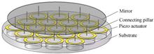
Adaptive optics system can detect the wavefront distortion of the optical system in real time and then control the mirror deformation of a deformable mirror to compensate the wavefront aberrations, so that the optical system can reach or approach the diffraction limit. It plays an important role in the fields of astronomical imaging, visual science and high-energy laser. Deformable mirrors driven by piezoelectric materials are widely used in the adaptive optics systems due to their high driving force and fast response. Piezoelectric deformable mirrors can be divided into two categories. One is the piezoelectric actuator array deformable mirror which is driven by the discrete piezoelectric actuators through the connecting pillars to deform the thin mirror. It is mainly used for the applications which require high number of actuators and high correction bandwidth. The other one is the bimorph deformable mirror which is composed of one or more piezoelectric layers bonded with the mirror layer. The transverse piezoelectric effect of piezoelectric materials is used to drive the mirror to produce bending deformation. Bimorph deformable mirror has a high interactuator coupling value and a strong correction capability for low-order aberrations. The traditional piezoelectric actuator array deformable mirror is driven by stack piezoelectric actuators, which has the advantages of large deformation and high resonant frequency. However, the high price limits its applications. Chengdu Institute of Optoelectronics Technology of Chinese Academy of Sciences and Xinetics Company improved the actuator structure with transverse piezoelectric effect to improve the actuator density of the deformable mirror and promote the compactness of the overall system design. However, the manufacturing process is complicated and is mainly applied in the astronomical field. In order to reduce the cost, OKO Technologies has proposed a deformable mirror driven by piezoelectric ceramic tubes which are cheaper than traditional stacked actuators. The price is still expensive. In addition, YANG E H and Ma Jianqiang proposed a deformation mirror driven by piezoelectric thin film and piezoelectric thick film array of micro-piezoelectric actuators, respectively. These deformable mirrors have the advantages of low drive voltage and large stroke. However, the manufacturing process of such deformation mirrors using micro-machining technology is complicated. This kind of deformation mirror is still in the stage of principle prototype. In order to further reduce the cost of deformable mirror with piezoelectric actuator array, a low-cost deformable mirror driven by piezoelectric unimorph actuator array is proposed in this paper. The deformable mirror comprises a mirror, a piezoelectric unimorph actuator array, connecting pillars and a substrate. The piezoelectric unimorph actuators are hexagonally arranged on the substrate with corresponding through holes. The piezoelectric unimorph actuator consists of a copper layer and a piezoelectric layer with both sides covered by electrodes. When a voltage is applied to the piezoelectric actuator, the actuator bents due to the transverse piezoelectric effect. The out of plane displacement of the actuator is transmitted to the mirror through the connecting pillar fixed at the center of the piezoelectric unimorph actuator, resulting in the deformation of the mirror. When all the piezoelectric actuators work together, the mirror can produce a conjugate shape with the distorted wavefront to compensate the wavefront aberrations. A deformable mirror prototype with 19 actuators and an effective pupil of 50 mm was fabricated. The piezoelectric unimorph actuator is commercially available, which is made of a brass disc and a piezoelectric ceramic disc bonded together with the diameters of 15 mm and 11 mm, and the thickness of 80 μm and 70 μm, respectively. The substrate material is optical quartz glass with 19 through holes. The mirror is a 3-inch single crystal silicon wafer with a thickness of 350 μm. Since the materials used are all commercially available and the manufacturing process is relatively simple, the cost of the proposed deformable mirror is much lower than other types of piezoelectric actuator array deformable mirrors (especially the stacked piezoelectric deformable mirrors). In order to verify the performances of deformable mirror driven by piezoelectric unimorph actuator array, an adaptive optics test system based on Shack-Hartmann sensor is built. A microlens array with 33×33 lenses is used for the measurement. Sixty-five Zernike polynomials are used for wavefront aberration fitting. The characteristics of actuator stroke, correction performance, mirror performance and frequency response are performed experimentally. The experimental results show that the wavefront deformation of a single actuator of the fabricated deformable mirror can reach 10 μm under a voltage of 50 V. The deformable mirror can accurately reconstruct the first 14-term Zernike polynomial aberrations. The far-field spot after correction is close to the Airy disc. The first-order natural frequency of the deformable mirror can reach 1.8 kHz. Compared to the traditional piezoelectric actuator array deformation mirror, this deformation mirror has the advantages of large stroke, low working voltage and low cost. The actuator number can be further increased for the implementation of the deformation mirror with large diameter and high number of actuators. The proposed deformable mirror has a promising application in the low-cost adaptive optics systems and even in astronomical imaging applications. Adaptive optics system can detect the wavefront distortion of the optical system in real time and then control the mirror deformation of a deformable mirror to compensate the wavefront aberrations, so that the optical system can reach or approach the diffraction limit. It plays an important role in the fields of astronomical imaging, visual science and high-energy laser. Deformable mirrors driven by piezoelectric materials are widely used in the adaptive optics systems due to their high driving force and fast response. Piezoelectric deformable mirrors can be divided into two categories. One is the piezoelectric actuator array deformable mirror which is driven by the discrete piezoelectric actuators through the connecting pillars to deform the thin mirror. It is mainly used for the applications which require high number of actuators and high correction bandwidth. The other one is the bimorph deformable mirror which is composed of one or more piezoelectric layers bonded with the mirror layer. The transverse piezoelectric effect of piezoelectric materials is used to drive the mirror to produce bending deformation. Bimorph deformable mirror has a high interactuator coupling value and a strong correction capability for low-order aberrations. The traditional piezoelectric actuator array deformable mirror is driven by stack piezoelectric actuators, which has the advantages of large deformation and high resonant frequency. However, the high price limits its applications. Chengdu Institute of Optoelectronics Technology of Chinese Academy of Sciences and Xinetics Company improved the actuator structure with transverse piezoelectric effect to improve the actuator density of the deformable mirror and promote the compactness of the overall system design. However, the manufacturing process is complicated and is mainly applied in the astronomical field. In order to reduce the cost, OKO Technologies has proposed a deformable mirror driven by piezoelectric ceramic tubes which are cheaper than traditional stacked actuators. The price is still expensive. In addition, YANG E H and Ma Jianqiang proposed a deformation mirror driven by piezoelectric thin film and piezoelectric thick film array of micro-piezoelectric actuators, respectively. These deformable mirrors have the advantages of low drive voltage and large stroke. However, the manufacturing process of such deformation mirrors using micro-machining technology is complicated. This kind of deformation mirror is still in the stage of principle prototype. In order to further reduce the cost of deformable mirror with piezoelectric actuator array, a low-cost deformable mirror driven by piezoelectric unimorph actuator array is proposed in this paper. The deformable mirror comprises a mirror, a piezoelectric unimorph actuator array, connecting pillars and a substrate. The piezoelectric unimorph actuators are hexagonally arranged on the substrate with corresponding through holes. The piezoelectric unimorph actuator consists of a copper layer and a piezoelectric layer with both sides covered by electrodes. When a voltage is applied to the piezoelectric actuator, the actuator bents due to the transverse piezoelectric effect. The out of plane displacement of the actuator is transmitted to the mirror through the connecting pillar fixed at the center of the piezoelectric unimorph actuator, resulting in the deformation of the mirror. When all the piezoelectric actuators work together, the mirror can produce a conjugate shape with the distorted wavefront to compensate the wavefront aberrations. A deformable mirror prototype with 19 actuators and an effective pupil of 50 mm was fabricated. The piezoelectric unimorph actuator is commercially available, which is made of a brass disc and a piezoelectric ceramic disc bonded together with the diameters of 15 mm and 11 mm, and the thickness of 80 μm and 70 μm, respectively. The substrate material is optical quartz glass with 19 through holes. The mirror is a 3-inch single crystal silicon wafer with a thickness of 350 μm. Since the materials used are all commercially available and the manufacturing process is relatively simple, the cost of the proposed deformable mirror is much lower than other types of piezoelectric actuator array deformable mirrors (especially the stacked piezoelectric deformable mirrors). In order to verify the performances of deformable mirror driven by piezoelectric unimorph actuator array, an adaptive optics test system based on Shack-Hartmann sensor is built. A microlens array with 33×33 lenses is used for the measurement. Sixty-five Zernike polynomials are used for wavefront aberration fitting. The characteristics of actuator stroke, correction performance, mirror performance and frequency response are performed experimentally. The experimental results show that the wavefront deformation of a single actuator of the fabricated deformable mirror can reach 10 μm under a voltage of 50 V. The deformable mirror can accurately reconstruct the first 14-term Zernike polynomial aberrations. The far-field spot after correction is close to the Airy disc. The first-order natural frequency of the deformable mirror can reach 1.8 kHz. Compared to the traditional piezoelectric actuator array deformation mirror, this deformation mirror has the advantages of large stroke, low working voltage and low cost. The actuator number can be further increased for the implementation of the deformation mirror with large diameter and high number of actuators. The proposed deformable mirror has a promising application in the low-cost adaptive optics systems and even in astronomical imaging applications.
Acta Photonica Sinica
- Publication Date: Jan. 25, 2022
- Vol. 51, Issue 1, 0151125 (2022)
Metamaterial Absorber with Tunable Absorption Bandwidth Based on Vanadium Dioxide
Xiaowei JIANG, Sheng WANG, and Hua WU
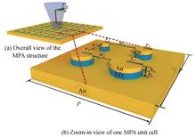
Metamaterial Perfect Absorber (MPA) is currently a research hotspot because of its numerous advantages such as high absorption efficiency, ultra-thin thickness, simple structure and so on. Since Landy et al. first proposed an MPA with perfect absorption characteristics, different types of MPAs have been proposed, and the absorption wavelengths over microwave, terahertz, infrared, and visible bands have been identified. However, once the structural parameters of MPA are fixed, the absorption bandwidth of MPA almost cannot be dynamically adjusted, which will limit its applications in some particular fields. This paper proposes a bandwidth-tunable MPA which is composed of vanadium dioxide (VO2) and Au. The research group simulated and analyzed the MPA based on Finite Difference Time Domain (FDTD) method. In the simulation, a periodic boundary condition was added in x- and y-directions, and a perfect match layer was added in the z-direction as the boundary condition. The polarization of the incident light was set to be TM polarization (Along the x axis). Incident light was perpendicular to the surface of the structure, which indicated the incident angle θ is 0. The simulation results show that the tuning range of absorption bandwidth can achieve 0.378 μm by controlling the temperature of VO2, and the absorption wavelength of MPA covered visible and near-infrared light. To explore the physical explanation for the high absorption efficiency in different wavelengths, we analyzed electromagnetic field distribution in MPA in different wavelengths, and revealed that although the high absorption efficiency is caused by the incident-light-stimulated surface plasmons in MPA, the working mechanism in visible and near infrared wavelength is quite different. In visible light range, no matter vanadium dioxide is in metallic state or dielectric state, the high absorption efficiency is caused by Propagating Surface Plasmon (PSP). On the other hand, for near-infrared light, if vanadium dioxide is in dielectric state, the high absorption efficiency is due to the Localized Surface Plasmon (LSP); or if vanadium dioxide is in metallic state, the high absorption efficiency is due to Fabry-Perot (FP) cavity resonance. Our results show that the MPA has the potential to be used in applications such as optical integrated devices and thermal emitters. Metamaterial Perfect Absorber (MPA) is currently a research hotspot because of its numerous advantages such as high absorption efficiency, ultra-thin thickness, simple structure and so on. Since Landy et al. first proposed an MPA with perfect absorption characteristics, different types of MPAs have been proposed, and the absorption wavelengths over microwave, terahertz, infrared, and visible bands have been identified. However, once the structural parameters of MPA are fixed, the absorption bandwidth of MPA almost cannot be dynamically adjusted, which will limit its applications in some particular fields. This paper proposes a bandwidth-tunable MPA which is composed of vanadium dioxide (VO2) and Au. The research group simulated and analyzed the MPA based on Finite Difference Time Domain (FDTD) method. In the simulation, a periodic boundary condition was added in x- and y-directions, and a perfect match layer was added in the z-direction as the boundary condition. The polarization of the incident light was set to be TM polarization (Along the x axis). Incident light was perpendicular to the surface of the structure, which indicated the incident angle θ is 0. The simulation results show that the tuning range of absorption bandwidth can achieve 0.378 μm by controlling the temperature of VO2, and the absorption wavelength of MPA covered visible and near-infrared light. To explore the physical explanation for the high absorption efficiency in different wavelengths, we analyzed electromagnetic field distribution in MPA in different wavelengths, and revealed that although the high absorption efficiency is caused by the incident-light-stimulated surface plasmons in MPA, the working mechanism in visible and near infrared wavelength is quite different. In visible light range, no matter vanadium dioxide is in metallic state or dielectric state, the high absorption efficiency is caused by Propagating Surface Plasmon (PSP). On the other hand, for near-infrared light, if vanadium dioxide is in dielectric state, the high absorption efficiency is due to the Localized Surface Plasmon (LSP); or if vanadium dioxide is in metallic state, the high absorption efficiency is due to Fabry-Perot (FP) cavity resonance. Our results show that the MPA has the potential to be used in applications such as optical integrated devices and thermal emitters.
Acta Photonica Sinica
- Publication Date: Jan. 25, 2022
- Vol. 51, Issue 1, 0151124 (2022)
Detect the Orbital Angular Momentum of Vortex Beams after Phase Distortion Based on Machine Learning
Chenyin SHI, Hongyan WEI, Peng JIA, and Xinyu YUE
Vortex beams carrying orbital angular momentum can be used in free space optical communication and have greater data coding freedom. However, the atmospheric turbulence channel is the key factor that limits the performance of vortex free space optical communication. It carries different random disturbances of the Laguerre Gaussian beam wavefront phase with orbital angular momentum modes, so it cannot keep its original orthogonality; it may cause serious signal crosstalk and receive light signal phases and intensities of ups and downs. When the vortex beams carrying information are transmitted in the atmospheric channel, it will be disturbed by turbulence and cause phase distortion. Vortex beam orbital angular momentum detection methods mainly include optical methods and machine learning methods. However, the optical method needs to use more communication system elements, the operation is complicated and the detection of vortex beams with phase disturbance is not involved. At the same time, the current machine learning methods have not involved the detection of high range orbital angular momentum modes so far, and need to know the prior knowledge of atmospheric turbulence. Aiming at the problem of measuring the orbital angular momentum mode information of vortex beams after phase distortion, this paper proposes a method to detect the orbital angular momentum mode information of vortex beams disturbed by atmospheric turbulence by using the designed convolutional neural network. A turbulence model of anisotropic atmospheric turbulence is established based on the multiphase screening method. Laguerre Gaussian beams with different beam parameters are transmitted in the simulated turbulence channel, and the intensity image of the Laguerre Gaussian vortex beam with phase distortion is obtained at the receiver end. In addition, the size of the receiver plate is fixed, and different sizes of the receiver plate are used to receive vortex beams with different ranges of orbital angular momentum. Due to the randomness of atmospheric turbulence, 10 vortex light intensity images under atmospheric turbulence were randomly simulated as data sets to make the model universally adaptable. To achieve better recognition performance, a convolutional neural network structure was optimized, and the orbital angular momentum recognition model based on a convolutional neural network was designed with 12 layers. In this method, the phase-distorted Laguerre Gaussian vortex beam intensity image is input as sample data. The network uses the input data set for independent learning, and after multiple iterations, it can accurately detect the high range of orbital angular momentum information of the beam. The simulation results show that when the intensity of atmospheric turbulence is uncertain, the accuracy of the model for the detection of vortex beams with orbital angular momentum modes of 1~40, 1~100, and 1~160 is as high as 94%, 90%, and 86%, respectively. For the vortex beam with orbital angular momentum mode 100, the accuracy of detection after 1 km, 2 km, 3 km and 4 km reaches 90%, 80%, 79% and 78%, respectively. When the radial index p is 0, 1, 2 and 3, the recognition accuracy is 90%, 85%, 80% and 79%, respectively. When the waist radius was 0.02, 0.03, 0.04 and 0.05, the model recognition accuracy was 90%, 87%, 83% and 82%, respectively. When the wavelength is 1550 nm, 1310 nm and 850 nm, the recognition accuracy is 90%, 88% and 86%, respectively. The proposed method has high accuracy and learning efficiency, and there is no need to convert the scroll beam into a beacon beam before detection, which reduces the number of components in the communication system, greatly reduces the complexity of the system and improves the detection rate of the scroll beam. The research results are of great significance for the application of scroll optical communication systems. Vortex beams carrying orbital angular momentum can be used in free space optical communication and have greater data coding freedom. However, the atmospheric turbulence channel is the key factor that limits the performance of vortex free space optical communication. It carries different random disturbances of the Laguerre Gaussian beam wavefront phase with orbital angular momentum modes, so it cannot keep its original orthogonality; it may cause serious signal crosstalk and receive light signal phases and intensities of ups and downs. When the vortex beams carrying information are transmitted in the atmospheric channel, it will be disturbed by turbulence and cause phase distortion. Vortex beam orbital angular momentum detection methods mainly include optical methods and machine learning methods. However, the optical method needs to use more communication system elements, the operation is complicated and the detection of vortex beams with phase disturbance is not involved. At the same time, the current machine learning methods have not involved the detection of high range orbital angular momentum modes so far, and need to know the prior knowledge of atmospheric turbulence. Aiming at the problem of measuring the orbital angular momentum mode information of vortex beams after phase distortion, this paper proposes a method to detect the orbital angular momentum mode information of vortex beams disturbed by atmospheric turbulence by using the designed convolutional neural network. A turbulence model of anisotropic atmospheric turbulence is established based on the multiphase screening method. Laguerre Gaussian beams with different beam parameters are transmitted in the simulated turbulence channel, and the intensity image of the Laguerre Gaussian vortex beam with phase distortion is obtained at the receiver end. In addition, the size of the receiver plate is fixed, and different sizes of the receiver plate are used to receive vortex beams with different ranges of orbital angular momentum. Due to the randomness of atmospheric turbulence, 10 vortex light intensity images under atmospheric turbulence were randomly simulated as data sets to make the model universally adaptable. To achieve better recognition performance, a convolutional neural network structure was optimized, and the orbital angular momentum recognition model based on a convolutional neural network was designed with 12 layers. In this method, the phase-distorted Laguerre Gaussian vortex beam intensity image is input as sample data. The network uses the input data set for independent learning, and after multiple iterations, it can accurately detect the high range of orbital angular momentum information of the beam. The simulation results show that when the intensity of atmospheric turbulence is uncertain, the accuracy of the model for the detection of vortex beams with orbital angular momentum modes of 1~40, 1~100, and 1~160 is as high as 94%, 90%, and 86%, respectively. For the vortex beam with orbital angular momentum mode 100, the accuracy of detection after 1 km, 2 km, 3 km and 4 km reaches 90%, 80%, 79% and 78%, respectively. When the radial index p is 0, 1, 2 and 3, the recognition accuracy is 90%, 85%, 80% and 79%, respectively. When the waist radius was 0.02, 0.03, 0.04 and 0.05, the model recognition accuracy was 90%, 87%, 83% and 82%, respectively. When the wavelength is 1550 nm, 1310 nm and 850 nm, the recognition accuracy is 90%, 88% and 86%, respectively. The proposed method has high accuracy and learning efficiency, and there is no need to convert the scroll beam into a beacon beam before detection, which reduces the number of components in the communication system, greatly reduces the complexity of the system and improves the detection rate of the scroll beam. The research results are of great significance for the application of scroll optical communication systems.
Acta Photonica Sinica
- Publication Date: Jan. 25, 2022
- Vol. 51, Issue 1, 0151123 (2022)
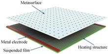
Study on Metasurface Ultra-narrowband Infrared MEMS Light Source
Yu ZOU, Wenjing JIANG, and Wen OU
Devices which meet needs, low cost, miniaturization, low power consumption and so on, has become one of future research directions with the development of the Internet of Things. The development of MEMS technology has made infrared light sources take an important step in miniaturization and low power consumption. In gas sensors, chemical detection and other fields, infrared light sources are required to have a single frequency band, so that the component concentration sensitive to the corresponding wavelength can be identified more accurately. However, the commonly used MEMS infrared light sources are gray body light sources, which have a relatively wide emission spectrum and a relatively low emissivity. A narrow-band, high-emissivity light source can not only improve the sensitivity of detection, but also increase the photoelectric conversion rate and reduce power consumption. Recently the main method to improve the performance of MEMS infrared light source is to attach a layer of micro nano structure on the surface of the light source, which mainly includes nano-silicon structure, photonic crystal, grating, etc. Nano-silicon structure can significantly increase the emissivity, but its spectral distribution range is still wide. Due to their nonresonant nature photonic crystal emitters do not have very sharp bands or high emissivity and therefore do not significantly increase efficiencies. Grating can also achieve selective emission, however its bandwidth is slightly wider. To solve this problem, A metasurface structure based on surface plasmon is proposed in this paper. This metasurface is mainly composed of metal-insulator-metal, and the top layer is a layer of metal with a patterned cross structure. This structure has an electromagnetic resonance response to light, and the electrical response can be achieved by the fine metal periodic array on the top layer. And the size of the material structure can be designed to achieve a magnetic response to electromagnetic waves in the infrared band. When light propagates to the surface of this structure, a part of it will cause a collective oscillation of electrons and photons which is called surface plasmons. When the metasurface is covered on the MEMS light source, the electromagnetic waves of the same frequency propagated by the thermal radiation of the MEMS heating module will resonate and radiate in the metasurface and the electromagnetic waves of other frequency will be reflected by the underlying metal layer. A Narrowband light source with selectivity and high emissivity based on metasurface is made by this principle. Fortunately, the metasurface is perfectly compatible with current CMOS and MEMS processes. However, Previous models do not distinguish metasurface of different shapes so as to have no reference value to design the metasurface. So the design of metasurface is only determined by time-consuming numerical optimization. To make the design more easily, An improved lumped equivalent circuit model is proposed in this paper, which base on the equivalent circuit theory and equivalent impedance theory. The response of the cross-shaped metasurface to light is converted into a circuit composed of resistance, inductance, and capacitance for analysis in this paper. And the circuit mainly includes the resistance, inductance, and mutual inductance and capacitance of the upper and underlying metals. The impedance of the model is analyzed to obtain the information of light frequency, bandwidth and so on according to the impedance matching theory of electromagnetic waves. Then the influence of the structure size on the center frequency, bandwidth and emissivity of the light source can be calculated accurately. The influence of the change of each size in the structure on the performance of the light source is explored by changing a single variable through the control variable method, and the influence of the change of the corresponding size in the model on the light source is also analyzed. The laws they reflect are basically the same. Using the model, A light source with a wavelength of 4 μm, an emissivity up to 99.7%, and a bandwidth of only 87 nm is be designed. The emission spectrum calculated by the model is basically consistent with the simulation results, which proves the predictability of the model, and at the same time it is also testified time-consuming and complex numerical optimization can be avoid during design by using the model. Devices which meet needs, low cost, miniaturization, low power consumption and so on, has become one of future research directions with the development of the Internet of Things. The development of MEMS technology has made infrared light sources take an important step in miniaturization and low power consumption. In gas sensors, chemical detection and other fields, infrared light sources are required to have a single frequency band, so that the component concentration sensitive to the corresponding wavelength can be identified more accurately. However, the commonly used MEMS infrared light sources are gray body light sources, which have a relatively wide emission spectrum and a relatively low emissivity. A narrow-band, high-emissivity light source can not only improve the sensitivity of detection, but also increase the photoelectric conversion rate and reduce power consumption. Recently the main method to improve the performance of MEMS infrared light source is to attach a layer of micro nano structure on the surface of the light source, which mainly includes nano-silicon structure, photonic crystal, grating, etc. Nano-silicon structure can significantly increase the emissivity, but its spectral distribution range is still wide. Due to their nonresonant nature photonic crystal emitters do not have very sharp bands or high emissivity and therefore do not significantly increase efficiencies. Grating can also achieve selective emission, however its bandwidth is slightly wider. To solve this problem, A metasurface structure based on surface plasmon is proposed in this paper. This metasurface is mainly composed of metal-insulator-metal, and the top layer is a layer of metal with a patterned cross structure. This structure has an electromagnetic resonance response to light, and the electrical response can be achieved by the fine metal periodic array on the top layer. And the size of the material structure can be designed to achieve a magnetic response to electromagnetic waves in the infrared band. When light propagates to the surface of this structure, a part of it will cause a collective oscillation of electrons and photons which is called surface plasmons. When the metasurface is covered on the MEMS light source, the electromagnetic waves of the same frequency propagated by the thermal radiation of the MEMS heating module will resonate and radiate in the metasurface and the electromagnetic waves of other frequency will be reflected by the underlying metal layer. A Narrowband light source with selectivity and high emissivity based on metasurface is made by this principle. Fortunately, the metasurface is perfectly compatible with current CMOS and MEMS processes. However, Previous models do not distinguish metasurface of different shapes so as to have no reference value to design the metasurface. So the design of metasurface is only determined by time-consuming numerical optimization. To make the design more easily, An improved lumped equivalent circuit model is proposed in this paper, which base on the equivalent circuit theory and equivalent impedance theory. The response of the cross-shaped metasurface to light is converted into a circuit composed of resistance, inductance, and capacitance for analysis in this paper. And the circuit mainly includes the resistance, inductance, and mutual inductance and capacitance of the upper and underlying metals. The impedance of the model is analyzed to obtain the information of light frequency, bandwidth and so on according to the impedance matching theory of electromagnetic waves. Then the influence of the structure size on the center frequency, bandwidth and emissivity of the light source can be calculated accurately. The influence of the change of each size in the structure on the performance of the light source is explored by changing a single variable through the control variable method, and the influence of the change of the corresponding size in the model on the light source is also analyzed. The laws they reflect are basically the same. Using the model, A light source with a wavelength of 4 μm, an emissivity up to 99.7%, and a bandwidth of only 87 nm is be designed. The emission spectrum calculated by the model is basically consistent with the simulation results, which proves the predictability of the model, and at the same time it is also testified time-consuming and complex numerical optimization can be avoid during design by using the model.
Acta Photonica Sinica
- Publication Date: Jan. 25, 2022
- Vol. 51, Issue 1, 0151122 (2022)

Effect on the Optical Properties of Planar Microlens Arrays with Different Ion-exchange Time
Yimunan XIE, Xiaoping JIANG, Sumei ZHOU, and Zhe YUAN
The plane microlens array is a plane array that is buried under the surface of the flat glass substrate,which consists of several microlens elements with uniform geometric dimensions and a three-dimensional gradient of refractive index according to a certain rule. There are many methods for making GRIN planar microlens arrays, including hot embossing technology, ion beam etching, the melted photoresist method, and so on. Each of these methods has certain advantages and limitations. The hot embossing technology has high pattern reproduction accuracy, but the demolding process is complicated. Using ion beam etching to fabricate microlens has good surface microstructure, but the production cost is high and production efficiency is low. The melted photoresist method has a simple manufacturing process, but the planar microlens array made by this method has poor thermal stability and is prone to aging. The fabrication process of GRIN planar microlens array using ion-exchanging method is relatively simple. The size of the lens element fabricated by ion-exchanging method can be less than 10 μm, the focal length can be less than 0.1 mm, and the thickness can be less than 0.1 mm. Moreover, the array structure and imaging uniformity are good. It has been widely used in artificial intelligence, portable equipment, integrated imaging, three-dimensional imaging, beam homogenization, beam shaping and other fields that require small-sized array optical elements. In this paper, circular aperture gradient index plane microlens arrays with different diameters are fabricated by ion-exchange technology and photolithography. By sampling in 6 time intervals during the ion-exchange process, the ion-exchanging depth and width of microlenses with different aperture sizes, the focal length, distortion and numerical aperture of lens elements were measured. The ratio of ion-exchange width to depth decreases with the increase of ion-exchange time, and the average diffusion rate of ions in the z-direction and r-direction gradually decreases. Moreover, that decreases faster for the flat microlens array with small opening diameter. As the ion-exchanging time increases, the focal lengths of the microlens arrays with two apertures gradually become shorter, and the focal lengths of the smaller aperture diameters are relatively shorter. The numerical aperture of the planar microlens arrays with different aperture diameters increases while the ion-exchange time increases, and its distortion decreases with the increase of ion exchange time. The rule that the optical characteristics of the gradient index planar microlens array changes with the ion-exchange time provides a reference for the production of the planar microlens array required in different optical systems. The plane microlens array is a plane array that is buried under the surface of the flat glass substrate,which consists of several microlens elements with uniform geometric dimensions and a three-dimensional gradient of refractive index according to a certain rule. There are many methods for making GRIN planar microlens arrays, including hot embossing technology, ion beam etching, the melted photoresist method, and so on. Each of these methods has certain advantages and limitations. The hot embossing technology has high pattern reproduction accuracy, but the demolding process is complicated. Using ion beam etching to fabricate microlens has good surface microstructure, but the production cost is high and production efficiency is low. The melted photoresist method has a simple manufacturing process, but the planar microlens array made by this method has poor thermal stability and is prone to aging. The fabrication process of GRIN planar microlens array using ion-exchanging method is relatively simple. The size of the lens element fabricated by ion-exchanging method can be less than 10 μm, the focal length can be less than 0.1 mm, and the thickness can be less than 0.1 mm. Moreover, the array structure and imaging uniformity are good. It has been widely used in artificial intelligence, portable equipment, integrated imaging, three-dimensional imaging, beam homogenization, beam shaping and other fields that require small-sized array optical elements. In this paper, circular aperture gradient index plane microlens arrays with different diameters are fabricated by ion-exchange technology and photolithography. By sampling in 6 time intervals during the ion-exchange process, the ion-exchanging depth and width of microlenses with different aperture sizes, the focal length, distortion and numerical aperture of lens elements were measured. The ratio of ion-exchange width to depth decreases with the increase of ion-exchange time, and the average diffusion rate of ions in the z-direction and r-direction gradually decreases. Moreover, that decreases faster for the flat microlens array with small opening diameter. As the ion-exchanging time increases, the focal lengths of the microlens arrays with two apertures gradually become shorter, and the focal lengths of the smaller aperture diameters are relatively shorter. The numerical aperture of the planar microlens arrays with different aperture diameters increases while the ion-exchange time increases, and its distortion decreases with the increase of ion exchange time. The rule that the optical characteristics of the gradient index planar microlens array changes with the ion-exchange time provides a reference for the production of the planar microlens array required in different optical systems.
Acta Photonica Sinica
- Publication Date: Jan. 25, 2022
- Vol. 51, Issue 1, 0151121 (2022)
Simulation of Generating Vortex Beam with Controllable Mode Based on Deformable Mirror with Continuous Surface
Ao TANG, Bin LAN, and Feng SHEN
High-power vortex lasers have good application prospects in optical processing and other fields. At present, most methods of generating vortex beams outside the cavity use phase-type devices, such as spiral phase plates and spatial light modulators, and these methods can not withstand high-power laser. The spiral mirrors can be used to generate high-power, but they can not flexibly modulate the vortex beam modes. Thus, the technology of generating mode-tunable high-power vortex beams is still a problem to be solve. In this paper, A method based on the Deformable Mirror (DM) with continuous surface to generate vortex beams is proposed. According to the helical symmetry phase of the vortex beam, the arrangement style of the actuators is designed as a ring, and by generating annular spiral wavefront to solve the DM can not fit singularity. Meanwhile, the annular spiral wavefront has the effect of suppressing side lobes. By comparing the mode purity of the annular spiral wavefront generating via the DM with different numbers drivers, the arrangement of driver arrays is determined, five rings and the number of drives in each ring from the inside to the outside is 15, 20, 25, 30, 35.Since the DM with continuous surface can not produce the ideal spiral wavefront, and the constant size beam used in simulation can not achieve the best effect of sidelobe suppression for the vortex beam with any mode. Therefore, there are high-frequency noise and high-order diffraction sidelobes in the vortex optical field generated by the DM designed. Hence, we add 4f filtering system to the optical path to remove they, and the expression of the radius of the main lobe of the vortex beam on the focal plane is derived as the radius of the filter hole. Finally, The sidelobe-free vortex beams with the topological charge equal to -5~5 are generated by simulation, whose amplitude distribution is a destructive ring, and the phase is quite close to the ideal spiral phase, furthermore, the mode purity is closed to 1 after filtering.The above results prove that the DM with continuous surface combined with the filter system can be used to generate a vortex beam with high mode purity. Moreover, the DM with continuous surface can flexibly generate different wavefront, and can withstand high-power laser, thus, this method has a good application prospect for generating high-power vortex beams with adjustable mode. High-power vortex lasers have good application prospects in optical processing and other fields. At present, most methods of generating vortex beams outside the cavity use phase-type devices, such as spiral phase plates and spatial light modulators, and these methods can not withstand high-power laser. The spiral mirrors can be used to generate high-power, but they can not flexibly modulate the vortex beam modes. Thus, the technology of generating mode-tunable high-power vortex beams is still a problem to be solve. In this paper, A method based on the Deformable Mirror (DM) with continuous surface to generate vortex beams is proposed. According to the helical symmetry phase of the vortex beam, the arrangement style of the actuators is designed as a ring, and by generating annular spiral wavefront to solve the DM can not fit singularity. Meanwhile, the annular spiral wavefront has the effect of suppressing side lobes. By comparing the mode purity of the annular spiral wavefront generating via the DM with different numbers drivers, the arrangement of driver arrays is determined, five rings and the number of drives in each ring from the inside to the outside is 15, 20, 25, 30, 35.Since the DM with continuous surface can not produce the ideal spiral wavefront, and the constant size beam used in simulation can not achieve the best effect of sidelobe suppression for the vortex beam with any mode. Therefore, there are high-frequency noise and high-order diffraction sidelobes in the vortex optical field generated by the DM designed. Hence, we add 4f filtering system to the optical path to remove they, and the expression of the radius of the main lobe of the vortex beam on the focal plane is derived as the radius of the filter hole. Finally, The sidelobe-free vortex beams with the topological charge equal to -5~5 are generated by simulation, whose amplitude distribution is a destructive ring, and the phase is quite close to the ideal spiral phase, furthermore, the mode purity is closed to 1 after filtering.The above results prove that the DM with continuous surface combined with the filter system can be used to generate a vortex beam with high mode purity. Moreover, the DM with continuous surface can flexibly generate different wavefront, and can withstand high-power laser, thus, this method has a good application prospect for generating high-power vortex beams with adjustable mode.
Acta Photonica Sinica
- Publication Date: Jan. 25, 2022
- Vol. 51, Issue 1, 0151120 (2022)
Design of Compact Polarization Beam Splitter Based on Triple-waveguide Directional Coupler
Dongmei ZHOU, Aihuan WANG, Cuiran LI, Xiaosuo WU, and Baowan YAN
In recent years, the silicon-on-insulator platform has attracted much interest in implementing integrated optical circuits. Due to the high refractive index contrast between the waveguide and cladding, the silicon-on-insulator waveguide has a strong light confinement ability, which helps the device to achieve a compact structure size and large-scale integration. However, this high refractive index contrast causes silicon nanophotonic devices to have high polarization sensitivity so that TE and TM modes have different propagation characteristics in an identical silicon-on-insulator waveguide, which may disrupt the optical signals in optical interconnections and quantum communications. To tackle this problem, one solution is using a polarization beam splitter to polarize the TM mode and TE mode light. Considering future ultra-dense photonic integrated circuits, a compact PBS with high performance is desired. Therefore, the hybrid plasma waveguide is introduced into the design of the polarization beam splitter. The hybrid plasmonic waveguide consists of a high refractive index dielectric layer (e.g., Si), a metal cap (e.g., Ag), and a thin low-index material layer (e.g., SiO2) between the Si layer and the metal layer. Compared with the traditional dielectric waveguide, it has a significant birefringence effect, which can maintain the performance of the device and further reduce the size of the device.In this paper, we propose and optimize a novel hybrid plasmonic polarization beam splitter utilizing asymmetrical directional coupling between the dielectric waveguides and a hybrid plasmonic waveguide on the silicon-on-insulator platform, which is ultracompact, and low-loss. Employing phase-matching conditions and super-mode theory, this polarization beam splitter is elaborately designed. The device is a three-waveguide asymmetric directional coupler. The middle hybrid plasmonic waveguide, which has a dielectric-loaded structure to enhance the refractive index contrast, is defined as the input waveguide. And different silicon-based waveguides on both sides are used to couple and separate TE and TM modes. Compared with the traditional polarization beam splitter based on the directional coupler composed of the same waveguide, this device facilitates two different types of waveguides to enhance the structural birefringence, which provides the device with an ultra-short coupling length and high extinction ratio. In addition, the dependence of TE and TM modes on the middle waveguide is also weakened.In this design of the device, it is necessary to ensure that the input waveguide and the TM coupling waveguide are phase-matched in the TM mode, but not phase-matched in the TE mode. In the case of the TE coupling waveguide, the principle of phase matching for TE mode is similar. The finite element method is used to calculate the mode field distribution and effective refractive index of silicon waveguides and a hybrid plasmonic waveguide, and then determine the size of each waveguide according to the phase matching conditions, which provides a basis for device modeling and simulation analysis. And the 3D finite difference time domain method is used to study the mode characteristics and optimize the structure of the polarization beam splitter to obtain better performance parameters. The experimental results show that the coupling lengths for TE and TM modes are 4.2 μm and 4.6 μm, respectively, and the polarization conversion efficiency of the modes can reach 94.7% and 95.5%, respectively. It can be seen from the light propagation of the polarization beam splitter that when the TE polarization mode is launched from the input side of the hybrid plasmonic waveguide, it is gradually coupled to the TE coupling port in the coupling region, with scarcely any modes mixing. Similarly, when the TM polarization mode is input into the hybrid plasmonic waveguide, it is finally coupled to the TM coupling port. For the TE mode, the polarization extinction ratio value is -38.9 dB and the insertion loss is -0.5 dB at the wavelength of 1.55 μm. For the wavelength range from 1.48 μm to 1.62 μm, the insertion loss of the TE mode is less than 0.92 dB, and the polarization extinction ratio is lower than -28.3 dB. For the TM mode, the polarization extinction ratio is -34.7dB, and the insertion loss is 0.45 dB at the wavelength of 1.55 μm. In the 140 nm wavelength range centered at 1.55 μm, the insertion loss of the TM mode is less than 0.89 dB, and the polarization extinction ratio is lower than -34.6 dB. The above experimental results mean that the performance of the polarization beam splitter is not sensitive to the wavelength. In addition, the influence of fabrication tolerance of waveguide in polarization beam splitter on device performance is also studied. Within the fabrication tolerance range of waveguides, the insertion loss of the mode is less than 2.8 dB, and the extinction ratio is lower than -22.5 dB. The results show that the device has high fabrication tolerances. In summary, the polarization beam splitter designed in this paper has a high extinction ratio, low insertion loss, and the coupling length is only 4.6 μm. It has great potential application value in the ultra-small silicon-based optical integrated circuits in the future. In recent years, the silicon-on-insulator platform has attracted much interest in implementing integrated optical circuits. Due to the high refractive index contrast between the waveguide and cladding, the silicon-on-insulator waveguide has a strong light confinement ability, which helps the device to achieve a compact structure size and large-scale integration. However, this high refractive index contrast causes silicon nanophotonic devices to have high polarization sensitivity so that TE and TM modes have different propagation characteristics in an identical silicon-on-insulator waveguide, which may disrupt the optical signals in optical interconnections and quantum communications. To tackle this problem, one solution is using a polarization beam splitter to polarize the TM mode and TE mode light. Considering future ultra-dense photonic integrated circuits, a compact PBS with high performance is desired. Therefore, the hybrid plasma waveguide is introduced into the design of the polarization beam splitter. The hybrid plasmonic waveguide consists of a high refractive index dielectric layer (e.g., Si), a metal cap (e.g., Ag), and a thin low-index material layer (e.g., SiO2) between the Si layer and the metal layer. Compared with the traditional dielectric waveguide, it has a significant birefringence effect, which can maintain the performance of the device and further reduce the size of the device.In this paper, we propose and optimize a novel hybrid plasmonic polarization beam splitter utilizing asymmetrical directional coupling between the dielectric waveguides and a hybrid plasmonic waveguide on the silicon-on-insulator platform, which is ultracompact, and low-loss. Employing phase-matching conditions and super-mode theory, this polarization beam splitter is elaborately designed. The device is a three-waveguide asymmetric directional coupler. The middle hybrid plasmonic waveguide, which has a dielectric-loaded structure to enhance the refractive index contrast, is defined as the input waveguide. And different silicon-based waveguides on both sides are used to couple and separate TE and TM modes. Compared with the traditional polarization beam splitter based on the directional coupler composed of the same waveguide, this device facilitates two different types of waveguides to enhance the structural birefringence, which provides the device with an ultra-short coupling length and high extinction ratio. In addition, the dependence of TE and TM modes on the middle waveguide is also weakened.In this design of the device, it is necessary to ensure that the input waveguide and the TM coupling waveguide are phase-matched in the TM mode, but not phase-matched in the TE mode. In the case of the TE coupling waveguide, the principle of phase matching for TE mode is similar. The finite element method is used to calculate the mode field distribution and effective refractive index of silicon waveguides and a hybrid plasmonic waveguide, and then determine the size of each waveguide according to the phase matching conditions, which provides a basis for device modeling and simulation analysis. And the 3D finite difference time domain method is used to study the mode characteristics and optimize the structure of the polarization beam splitter to obtain better performance parameters. The experimental results show that the coupling lengths for TE and TM modes are 4.2 μm and 4.6 μm, respectively, and the polarization conversion efficiency of the modes can reach 94.7% and 95.5%, respectively. It can be seen from the light propagation of the polarization beam splitter that when the TE polarization mode is launched from the input side of the hybrid plasmonic waveguide, it is gradually coupled to the TE coupling port in the coupling region, with scarcely any modes mixing. Similarly, when the TM polarization mode is input into the hybrid plasmonic waveguide, it is finally coupled to the TM coupling port. For the TE mode, the polarization extinction ratio value is -38.9 dB and the insertion loss is -0.5 dB at the wavelength of 1.55 μm. For the wavelength range from 1.48 μm to 1.62 μm, the insertion loss of the TE mode is less than 0.92 dB, and the polarization extinction ratio is lower than -28.3 dB. For the TM mode, the polarization extinction ratio is -34.7dB, and the insertion loss is 0.45 dB at the wavelength of 1.55 μm. In the 140 nm wavelength range centered at 1.55 μm, the insertion loss of the TM mode is less than 0.89 dB, and the polarization extinction ratio is lower than -34.6 dB. The above experimental results mean that the performance of the polarization beam splitter is not sensitive to the wavelength. In addition, the influence of fabrication tolerance of waveguide in polarization beam splitter on device performance is also studied. Within the fabrication tolerance range of waveguides, the insertion loss of the mode is less than 2.8 dB, and the extinction ratio is lower than -22.5 dB. The results show that the device has high fabrication tolerances. In summary, the polarization beam splitter designed in this paper has a high extinction ratio, low insertion loss, and the coupling length is only 4.6 μm. It has great potential application value in the ultra-small silicon-based optical integrated circuits in the future.
Acta Photonica Sinica
- Publication Date: Jan. 25, 2022
- Vol. 51, Issue 1, 0151119 (2022)
Holographic Phase Switch Based on Phase-change Metasurface
Zhihua FAN, Yufei WU, Xiaoyu MA, and Shaolin ZHOU
In priciple, metasurfaces for phase regulation based on the generalized Snell’s law enable arbitrary wavefront or spatial phase tuning via ultrathin interface with deep subwavelength thickness. Specifically, such ultrathin metasurfaces are essentially composed of anisotropic meta-elements that are eleborately arranged to achieve phase modulations pixelwisely in a subwavelength-level local manner in a full range covering [0 2π]. However, most current metasurfaces lack of the flexibility of active tuning due to their post-factication passive nature. In this situtations, the ultracompact reconfigurable devices with high-level of integration become highly desirable for a few applications such as the active photonic, optoelectronic integration and so on. Therefore, this paper aims to combine the actively tunable property of newly emerging phase change materials with the framework of metasurfaces with the functions of phase tuning based on the generalized Snell's law. As proof of concept, the far-field switchable holographic imaging is reasonably demonstrated acting as one type of meta-switch for certain scenarios of controllable hologram generation. In detail, the phase change material of germanium antimony telluride (Ge2Sb2Te5, “GST” in short) alloy is integrated into the meta-atom design for the essential switchable control. For the amorphous-GST integrated device incident by the circularly polarized wave, the predefined anisotropic meta-atoms can achieve broadband (1.55~2.8 μm) geometrical phase modulation with the polarization conversion ratio (PCR) up to ~80%, producing the near-field holographic phase distribution for the far-field holographic imaging, i.e. the “on” state for our device. However, upon the phase change of GST to its crystalline state, the PCR of meta-atoms is minimized and the holographic phase and image reconstruction are then switched off. As a result, the phase-type photonic switch proposed in this paper have great potentials in active photonic and optoelectronic integration such as the spatial light modulation, wavefront engineering, holographic imaging. In priciple, metasurfaces for phase regulation based on the generalized Snell’s law enable arbitrary wavefront or spatial phase tuning via ultrathin interface with deep subwavelength thickness. Specifically, such ultrathin metasurfaces are essentially composed of anisotropic meta-elements that are eleborately arranged to achieve phase modulations pixelwisely in a subwavelength-level local manner in a full range covering [0 2π]. However, most current metasurfaces lack of the flexibility of active tuning due to their post-factication passive nature. In this situtations, the ultracompact reconfigurable devices with high-level of integration become highly desirable for a few applications such as the active photonic, optoelectronic integration and so on. Therefore, this paper aims to combine the actively tunable property of newly emerging phase change materials with the framework of metasurfaces with the functions of phase tuning based on the generalized Snell's law. As proof of concept, the far-field switchable holographic imaging is reasonably demonstrated acting as one type of meta-switch for certain scenarios of controllable hologram generation. In detail, the phase change material of germanium antimony telluride (Ge2Sb2Te5, “GST” in short) alloy is integrated into the meta-atom design for the essential switchable control. For the amorphous-GST integrated device incident by the circularly polarized wave, the predefined anisotropic meta-atoms can achieve broadband (1.55~2.8 μm) geometrical phase modulation with the polarization conversion ratio (PCR) up to ~80%, producing the near-field holographic phase distribution for the far-field holographic imaging, i.e. the “on” state for our device. However, upon the phase change of GST to its crystalline state, the PCR of meta-atoms is minimized and the holographic phase and image reconstruction are then switched off. As a result, the phase-type photonic switch proposed in this paper have great potentials in active photonic and optoelectronic integration such as the spatial light modulation, wavefront engineering, holographic imaging.
Acta Photonica Sinica
- Publication Date: Jan. 25, 2022
- Vol. 51, Issue 1, 0151118 (2022)
Integrated Design of Optically Transparent Composite for Low Infrared Emission and Wideband Microwave Absorption Metasurface
Tong XIAO, Changhui TIAN, Cuilian XU, and Zhiqiang GAO
In recent years, metamaterials have attracted great attention in stealth technology. As a special two-dimensional metamaterial, hypersurface is more suitable for the design of infrared radar compatible stealth structures. Based on optically transparent materials Indium Tin Oxide (ITO), Polyethylene Terephthalate (PET) and Polymethyl Methacrylate (PMMA), an optically transparent infrared radar compatible stealth composite metasurface is realized by using the idea of integrated design of infrared low emission layer and radar absorbing layer. The structure consists of three parts: functional layer, dielectric layer, and reflective back plate, with a total thickness of only 1.17 mm. By etching the ITO pattern on the surface of the functional layer and optimizing the pattern size of the pattern, the broadband absorption higher than 90% in the frequency range of 15.9~35.1 GHz in the microwave band is realized. At the same time, the infrared emissivity is reduced by increasing the ITO duty cycle on the surface of the functional layer, and the infrared emissivity on the surface of the structure is controlled at 0.25. Based on the analysis of the surface current of the material, the mechanism of super surface absorbing wave is expounded, and the influence of different patches on the absorbing wave ability is analyzed. Through the analysis of surface current, it is found that almost only the small square patch in the middle and four large square patches around form the resonant structure, while the four rectangular patches and the peripheral square patches make little contribution to the resonant consumption. When the middle rectangular patch does not exist, the bandwidth absorbed by 90% of the high frequency part can be increased by nearly 5 GHz, but it also means that the proportion of ITO on the surface of the structure is reduced, which affects the infrared emissivity of the whole structure. Through simulation experiments, the changes of the absorbing capacity of the designed structure at different incident angles are discussed. For TE mode, the structure can maintain high absorptivity when the incident angle is less than 30°. With the further increase of the angle, the absorptivity of the low-frequency part decreases more. For TM mode, the absorptivity of the structure is only about 0.8 when the incident angle is small. With the increase of the incident angle to 35°, the structure can maintain 90% absorptivity in the range of 20.1~35.0 GHz. It shows that the absorbing ability of the structure at large incident angle in TM mode is stronger than that in TE mode. In order to further verify the simulation results, the conductive ITO film deposited on the optically transparent PET substrate was etched into the designed structure by laser etching technology, and the experimental sample was processed, the sample size was 360 mm×360 mm. The microwave absorption capacity, infrared emissivity and visible light transmittance of the sample were measured respectively. The microwave absorption performance is tested in the microwave darkroom. The measurement system is composed of Agilent N5224a network analyzer and three pairs of broadband horn antennas. During the measurement, the metal base plate with the same size is selected for normalization, and then the reflectivity is measured. After calculation, the absorption curve is obtained. Considering the square resistance and size error of ITO in sample processing, it is considered that the experimental results are basically consistent with the simulation results. The optical transparency performance is measured by ultraviolet visible spectrophotometer (model: uv-3600 plus). After calculation, the average visible light transmittance of the overall structure is about 0.704. The results effectively show that the designed integrated infrared radar compatible stealth composite hypersurface has good optical transparency performance in the visible band. For the infrared emissivity of the designed structure, Tss-5x infrared emissivity tester (spectral response range: 2~22 μm) and FTIR spectrometer are used to measure the emissivity of the sample. ITO film of 6.0 Ω/sq, pet substrate and material samples etched with ITO pattern are measured respectively. In order to ensure the effectiveness of the measured data, each material is measured at five different positions, and the obtained infrared emissivity is 0.246, which is very close to the average infrared emissivity of the designed material sample obtained by direct measurement of 0.248. The infrared emissivity of the sample with the designed structure in the range of 3.0~14.0 μm is measured by FTIR spectrometer, which is about 0.25, which is close to the theoretical calculation value and the measurement value obtained by Tss-5x infrared emissivity tester. It can be considered that the designed structure has better infrared stealth ability. The structure has thin thickness, good broadband radar absorption performance, low infrared emissivity and visible light transparency. In recent years, metamaterials have attracted great attention in stealth technology. As a special two-dimensional metamaterial, hypersurface is more suitable for the design of infrared radar compatible stealth structures. Based on optically transparent materials Indium Tin Oxide (ITO), Polyethylene Terephthalate (PET) and Polymethyl Methacrylate (PMMA), an optically transparent infrared radar compatible stealth composite metasurface is realized by using the idea of integrated design of infrared low emission layer and radar absorbing layer. The structure consists of three parts: functional layer, dielectric layer, and reflective back plate, with a total thickness of only 1.17 mm. By etching the ITO pattern on the surface of the functional layer and optimizing the pattern size of the pattern, the broadband absorption higher than 90% in the frequency range of 15.9~35.1 GHz in the microwave band is realized. At the same time, the infrared emissivity is reduced by increasing the ITO duty cycle on the surface of the functional layer, and the infrared emissivity on the surface of the structure is controlled at 0.25. Based on the analysis of the surface current of the material, the mechanism of super surface absorbing wave is expounded, and the influence of different patches on the absorbing wave ability is analyzed. Through the analysis of surface current, it is found that almost only the small square patch in the middle and four large square patches around form the resonant structure, while the four rectangular patches and the peripheral square patches make little contribution to the resonant consumption. When the middle rectangular patch does not exist, the bandwidth absorbed by 90% of the high frequency part can be increased by nearly 5 GHz, but it also means that the proportion of ITO on the surface of the structure is reduced, which affects the infrared emissivity of the whole structure. Through simulation experiments, the changes of the absorbing capacity of the designed structure at different incident angles are discussed. For TE mode, the structure can maintain high absorptivity when the incident angle is less than 30°. With the further increase of the angle, the absorptivity of the low-frequency part decreases more. For TM mode, the absorptivity of the structure is only about 0.8 when the incident angle is small. With the increase of the incident angle to 35°, the structure can maintain 90% absorptivity in the range of 20.1~35.0 GHz. It shows that the absorbing ability of the structure at large incident angle in TM mode is stronger than that in TE mode. In order to further verify the simulation results, the conductive ITO film deposited on the optically transparent PET substrate was etched into the designed structure by laser etching technology, and the experimental sample was processed, the sample size was 360 mm×360 mm. The microwave absorption capacity, infrared emissivity and visible light transmittance of the sample were measured respectively. The microwave absorption performance is tested in the microwave darkroom. The measurement system is composed of Agilent N5224a network analyzer and three pairs of broadband horn antennas. During the measurement, the metal base plate with the same size is selected for normalization, and then the reflectivity is measured. After calculation, the absorption curve is obtained. Considering the square resistance and size error of ITO in sample processing, it is considered that the experimental results are basically consistent with the simulation results. The optical transparency performance is measured by ultraviolet visible spectrophotometer (model: uv-3600 plus). After calculation, the average visible light transmittance of the overall structure is about 0.704. The results effectively show that the designed integrated infrared radar compatible stealth composite hypersurface has good optical transparency performance in the visible band. For the infrared emissivity of the designed structure, Tss-5x infrared emissivity tester (spectral response range: 2~22 μm) and FTIR spectrometer are used to measure the emissivity of the sample. ITO film of 6.0 Ω/sq, pet substrate and material samples etched with ITO pattern are measured respectively. In order to ensure the effectiveness of the measured data, each material is measured at five different positions, and the obtained infrared emissivity is 0.246, which is very close to the average infrared emissivity of the designed material sample obtained by direct measurement of 0.248. The infrared emissivity of the sample with the designed structure in the range of 3.0~14.0 μm is measured by FTIR spectrometer, which is about 0.25, which is close to the theoretical calculation value and the measurement value obtained by Tss-5x infrared emissivity tester. It can be considered that the designed structure has better infrared stealth ability. The structure has thin thickness, good broadband radar absorption performance, low infrared emissivity and visible light transparency.
Acta Photonica Sinica
- Publication Date: Jan. 25, 2022
- Vol. 51, Issue 1, 0151117 (2022)
Topics
© Copyright 2018-2021 | Chinese Laser Press. All Rights Reserved 沪ICP备15018463号-20